Capstone Design
Hardware-Based Video Controller and Graphics Processor Unit for a RISC-V processor.
Table of contents
- About
- Team and Team Structure
- Problem Statement
- Design Constraints
- Ethical and Professional Responsibilities
- Design Strategy
- Design Details
About
This documentation contains the contents of the final-deliverable my team presented for our Capstone Design project. We recieved the award for the ECE Best Senior Design Project from the ECE department at Oklahoma State University, as well as an A+ final grade.

Team and Team Structure
- Adam Loeckle : AHB Interconnect, Struct Implementation for the Multi-Manager System, Uncore modification
- Jacob Pease : AHB Interconnect, Round Robin Arbiter, Input Stage, Uncore modification
- Josh Minton : I2C Interface, Wally on VCU108 Evaluation Board
- McKain Box : Frame Buffer, HDMI Signal Generator, Top-Level Frame Processing Control, Wally on VCU108 Evaluation Board
Problem Statement
The goal of this project was to design a video display controller for Wally, a family of open-source RISCV processors, being jointly developed by Prof. David Harris’ Advanced Digital Design class at Harvey Mudd College and Prof. James Stine’s VLSI Computer Architecture Research Group at Oklahoma State University. To do this, the bus system Wally used needed to be expanded to a multi-master bus system. The individual components of the video display controller also needed to be implemented, such as the frame buffer, and HDMI transmitter. The design was made to be simulated on a field-programmable gate array (FPGA). The ultimate goal of making this video display controller would be to view the Linux operating system running on Wally on an FPGA through a monitor.
Design Constraints
Regulatory Requirements
The design of hardware using SystemVerilog, in the scope of this project, is not heavily regulated. As this will be open source, it is a mild consideration as to whether this will be mass-produced. The use of FPGA’s is regulated in other contexts, such as aircraft and nuclear safety systems.
Applicable Industry or Professional Standards
The Wally project and the wider RISC-V ecosystem are founded on an open-source philosophy. Wally aims to provide students and researchers with access to a modern processor without any licensing fees or requiring any expensive proprietary development toolchains. Our team incorporated this mindset into our design decisions, intending to make as much of our project as possible reusable by the Wally team. Proprietary components are only used for implementation-specific tasks, such as interfacing with our FPGA and its onboard HDMI transmitter. These components were modularized in a way that makes them easily removable in future work. Additionally, some non-free components were used in the interest of getting a working project within the timeframe but would have been replaced if given more time on the project. For example, we planned initially to use the DVI standard instead of the HDMI standard, which requires a license to use, because all HDMI displays are backward compatible with DVI-D, which does not.
Funding, Scheduling, Manpower, and Contractual Constraints
Funding
For our project, all the required components needed were supplied by Dr. Stine at no cost to our project. These parts include the VCU108 evaluation board, a desktop running Linux, a monitor which supports up to four video inputs, and static protection mats and wrist wraps. ModelSim and Xilinx Vivado software licenses were required for simulation and hardware testing, so we were able to obtain existing licenses through Dr. Stine’s research team at no additional cost. The total cost of our project was $0, therefore there was no constraint to our progress caused by funding.
Scheduling and Manpower Constraints
We had fifteen total weeks, including spring break, to complete this project, but during February, we lost an entire week’s worth of time caused by ice storms closing campus and some team members losing power. The primary scheduling constraint we endured was most of the team had jobs outside of capstone and other course work, or a family to take care of. Taking these constraints into consideration, we were able to frequently communicate and track progress using a Discord server.
Contractual Constraints
The only contractual constraint we had to follow was making sure every component qualifies as an open source due to the nature of RISC-V guidelines as a free and open instruction set architecture.
Applicable Issues of Public Health, Safety, and Welfare; and Cultural, Social, Environmental, and Economic Factors Influencing Design Choices and Trade-Offs
Our project contains zero health safety or environmental risks. The only environmental concern would be the power consumption of the FPGA and attached monitor. Since FPGAs are different from ASIC devices and how they can be fully programmable, the power consumption is dependent on the design running on the device.
Ethical and Professional Responsibilities
An ethical responsibility that we felt was important in influencing our design decisions was ensuring that we were not utilizing any intellectual properties. For example, the HDMI protocol. The Wally project’s goal is to be completely open source and using any licensed software or hardware would go against that.
Design Strategy
Phase 1: Research
The purpose of the initial phase of this project was to primarily research different topics that would aid in our work throughout the semester. This included general research of the RISCV architecture and FPGA designs, HDMI specifications, and AHB lite design requirements. We also gained access to the ECEN servers that were necessary for compiling and testing our additions to Wally.
This also included getting familiar with the Wally repository and gaining access to the tools needed to work on the project. This was necessary, especially for the creation of our Multi-Manager AHB, for understanding how the processor operated inside of Uncore and the present AHB lite system. We created branches from the Wally repository to be able to push, pull, and test our code without committing changes directly to the main branch.
Phase 2: Multi-Manager AHB
The focus of Phase 2 was to expand the single manager (master) bus implementation currently a part of Wally into a multi-manager bus system according to the AHB (Advanced High-performance Bus) spec. The reason for doing this was to allow our Video Display Controller to access the DDR4 memory on the FPGA concurrently with the CPU. In addition to expanding the bus system for our GPU, our goal was to generalize the multimanager system to be expandable for any number of managers or devices for the benefit of Wally. It should be noted that in the AHB bus specification [3], masters are referred to as managers, and slaves are referred to as subordinates.
Our design strategy was to encapsulate the 11 different AHB signals in structs and instantiate these signals based on the number of managers defined in the configuration files. Then, using a generate block inside “uncore.sv” (the module responsible for directing read and write requests to different subordinates), the necessary hardware for each Manager would be generated.
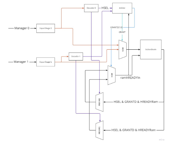
The section of hardware that is responsible for directing any single manager to the subordinate it’s trying to access is called the interconnect. [1] The interconnect is made up of several components in addition to the already existing components that are part of the single-manager system. In our multi-manager implementation, we’ve utilized the following components:
- An “input stage” for each manager.
- A Round Robin arbiter for each subordinate.
- A mux that gives the subordinate the correct manager signal
- A mux that gives the arbiter and the subordinate the correct HREADY signal.
- A mux to return the correct subordinate signals to the manager.
- Address decoders for each manager.
Below is a diagram of how two managers would access one subordinate, demonstrating the basic idea of how the interconnect works:
Phase 3: Video Controller
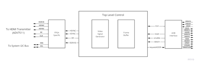
For phase three, we set out to create the video controller portion of the project. The video controller includes different components which are essential for the development of the final design. First, the frame buffer module is needed to control the input and output of pixel memory from the CPU by using read and write addressing and block random access memory. The size of the buffer is dependent based on the total size of the frame being presented. Secondly, an HDMI video signal generator is essential as it provides the HDMI transmitter with horizontal and vertical positioning to produce a video output from pixel data stored within the frame buffer.
When communicating with the HDMI transmitter chip, the output signals must be properly controlled based on the resolution size of the video frame using a top-level control module. Using syncing and porch timings, you will be able to display the following signals at the correct and expected intervals:
- HSYNC (Horizontal Sync)
- VSYNC (Vertical Sync)
- DE (Data Enable)
Third and finally an HDMI transmitter is needed to handle the TDMS packets and DDC interface and push the input data onto a screen. To control the transmitter, a board specific I2C controller is required. As seen below, you can see how each of these modules is connected:
Phase 4: FPGA Implementation
In the final phase of the project, both our design and the Wally processor needed to be implemented on an FPGA. The Xilinx VCU108 Evaluation board was used for this purpose. The HDMI transmitter on the VCU108 needs to be supplied with video resolution, timing, and color space information through a series of internal register writes through its I2C interface. We designed a custom I2C master to accomplish this. Finally, the Wally processor required additional configuration to the input clock speeds and the FPGA pin assignments to work on the VCU108.
Design Details
Multi-Manager System
Struct Package
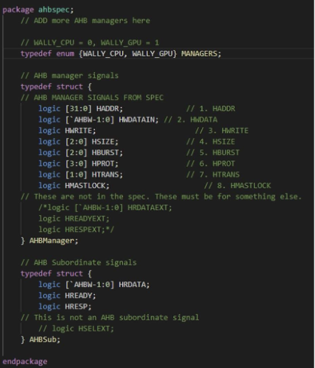
To allow for dynamic expansion of the AHB bus system to accommodate an arbitrary number of masters, we came up with a system to handle each AHB Manager (Master) and AHB Subordinate (Slave) device’s respective data signals accordingly across the platform. Given the large number of signals that are associated with these devices, we implemented a struct system. These structs are used in a dynamic array that is based on the number of managers that are defined globally for Wally. This will allow future users of the platform to add/change the number of managers with ease, making an expansion of the project agile.
Using this method of dynamic struct arrays allows for an easy method to add future managers to Wally. These struct definitions replace the input and output logic of the manager and subordinate signals in Uncore, the AHBlite bus, as well as higher-level modules in Wally that handle this manager and subordinate data. When implementing the full AHB interconnect inside of Uncore, these manager signals will be accessed by referencing the enumeration definition in the struct package. After this implementation, using only one manager (CPU), the Wally regression tests passed. Pictured below is the struct package definition:
Round Robin Arbiter
In a multi-manager (multi-master) system, in situations where more than one manager is trying to access the same subordinate, it’s important to be able to choose which manager is granted access first and in what order the other managers are granted access afterward. This prevents what is called “collisions” where one manager interferes with another manager’s attempts to read and write on the bus. This is called “arbitration”. In most bus systems there are two common methods of arbitration: fixed priority, and round-robin.
In fixed priority arbitration, each manager is assigned a certain priority. If a higher priority manager is granted access, the lower priority managers will have to wait until the higher priority manager is done. This is easy to implement but tends to leave other managers waiting for a long period. This is called “starvation”.
Round robin arbitration solves the “starvation” problem and is also easy to implement. Because of this, it is very common to see this method of arbitration in most bus systems. Round robin arbitration works by cyclically assigning the highest priority to each manager in turn. This means the longest a manager must wait for its request to be serviced is the number of managers minus one (M-1). This is the arbitration method we decided to implement in our bus system.
We based our implementation of the round-robin arbiter on a research paper [2] that uses a rotating bit shifter to shift the input signal depending on which manager a local pointer is currently pointing at. This rotated signal is then passed through a normal fixed priority arbiter and is then de-rotated to produce the correct grant signal. Below is a diagram of how this works:

The structure of the fixed priority arbiter between rotates is straightforward. It is a simple sequence of AND gates, where the input to a higher level AND gate is used to drive the outputs of the lower level AND gates low. Below is a screenshot of this code:
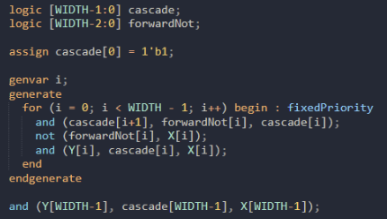
This module can generate any width fixed priority arbiter. All modules that are part of the interconnect are parameterized so that they can grow with the number of Managers.
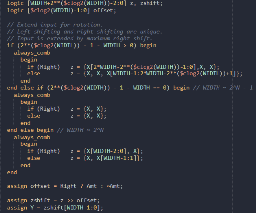
The rotator modules are based on the bit shifting code used as a part of Wally to do bit-shifting. However, this module was heavily modified so that it could generate a rotating bit shifter for any number, not just powers of two. To accomplish this, a complex series of equations was developed and used inside the rotator module. The key principle behind these equations was to extend the internal number of bits by the maximum possible shift minus one depending on the width of the shift amount, resulting in the following code:
The Arbiter itself was constructed by instantiating the necessary rotators and fixed priority arbiter.
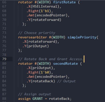
The GRANT signal is calculated immediately as HSELInternal changes. This is necessary to be ready to grant access to the appropriate manager if the highest priority manager requests access within a single clock cycle. Again, this module is parameterized to allow the arbiter to expand for any number of managers.
The way an arbiter classifies whether a manager is making a request is based on the HSEL signal (which is output by the decoders when a manager accesses a particular region of memory) and the manager’s own HTRANS signal, which represents the transfer state of the manager. Currently, Wally only implements two HTRANS states: IDLE, and NONSEQ. A manager is IDLE when it is not trying to make a request on the bus, and it changes to NONSEQ when it tries to make a “non-sequential” transfer. If the manager is selecting the subordinate as well as having a state of NONSEQ, then this manager is making a request.
The arbiter takes as an input the incoming select signals from all the managers as well as the HTRANS states of every manager. It then calculates HSELInternal from these two signals. This is calculated by the following code:
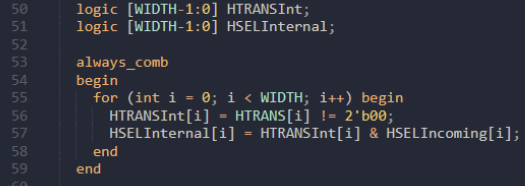
Another important feature of the arbiter is that it outputs two signals related to granting access. In addition to the primary “GRANT” signal, it outputs another signal labeled “GRANTD”. GRANT is used to determine which manager’s AHB signals the subordinate will receive. GRANTD is used to determine which manager is going to receive the data the subordinate supplies after one clock cycle or after it has “waited” the manager for a certain number of clock cycles.
When a subordinate waits for a manager, HREADY is set low. When HREADY goes high again it means two things: the data is ready to be sampled by the manager, and the subordinate is ready to receive the next request. In a multimanager system, however, a single HREADY could only mean the ending of the previous request for a particular manager, but managers don’t know that. If the manager wants to make a request immediately after HREADY goes high, the address it was trying to send through will need to be stored, otherwise, depending on how the manager sets up its AHB signals (ahblite.sv works differently than the spec), the interconnect will lose the request before it had a chance to deal with it. This topic will be dealt with more in the input stage section.
The grant signals can be understood like this: GRANT represents the beginning of a transfer, and GRANTD represents the end of a transfer. GRANTD is so labeled because it is a delayed version of GRANT, triggered by HREADY. When a manager’s GRANTD signal is high and the subordinate’s HREADY signal is high, this means it’s transfer is complete and the interconnect is ready to accept the next request. Thus, GRANTD becomes an essential signal for coordinating transfers inside the interconnect.
Input Stage
The input stage, as discussed in the arbiter section, is necessary for storing requests from managers when those managers get “waited”. [1] According to the specification, as soon as the request is sampled by the subordinate, the manager can progress to the next request. In the next clock cycle, or when HREADY goes high again, two things will happen. The subordinate will return the data for the previous request and the new request will get sampled. This can be seen in the diagram of a basic transfer from the AHB specification document:

However, as previously mentioned, when HREADY goes high for a specific manager in a multi-manager system, that may only represent the end of the previous transfer and not the start of the next one. Thus, in a multimanager system, if more than one manager is trying to access a particular subordinate, at the end of a transfer where one manager will lose access, it may try to progress to the address under the assumption that its current address will be sampled. Thus, the request will be lost completely, and a misread will occur.
To prevent this, an input stage is necessary per the AHB multimanager specification. This input stage will store incoming requests when managers are waited by the arbiter for the subordinate the managers are accessing. To accomplish this, a state machine was created inside the input stage module that handled when it was necessary to store certain values:
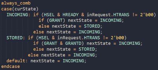
First, we must consider whether the manager is attempting to make a request and if the interconnect is ready to receive the request. Then, if the manager has been granted access, we can send the incoming request straight to the subordinate. However, if it has not been granted access, we want to store the value immediately, until it has been granted access.
In the STORED state, the only way to get out of it is if GRANT and GRANTD are both high. This means that the next HREADY is the beginning of a new transfer for this manager, thus we can go back to sending the incoming request to the subordinate. Otherwise, we remain in the STORED state.
When testing this input stage, we found that the output of ahblite.sv perfectly mimics what the input stage would output anyway. That’s because ahblite.sv is written to only change what address it’s requesting after it has received an HREADY of high. Though this does not break the functioning of the bus, it is not how the spec describes a manager.
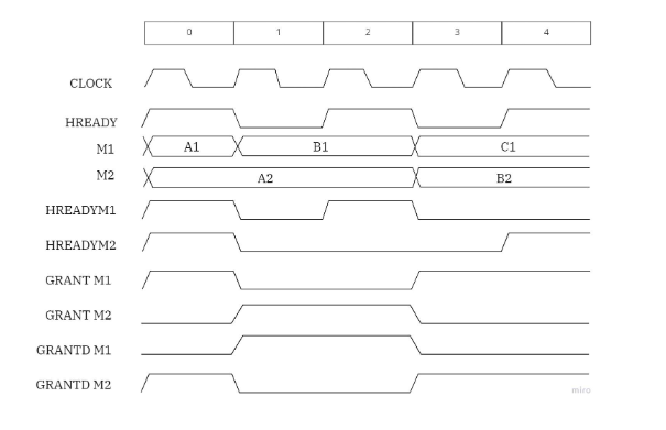
In our multimanager system, the ideal timing diagram for two managers that want to make transfers is shown below:
Interconnect
For this project, we did not instantiate an arbiter for every subordinate. We instantiated a single arbiter for the ram module, which is what our video display controller would have used to gather frame data. Since this was the only device the video display controller would need access to, this is the only one we included as part of the interconnect. However, due to the flexibility of our design, it would not be hard to expand the interconnect to include the other subordinates as well.
The interconnect is contained within “uncore.sv” and is instantiated using a generate block just before the subordinates are generated. For each manager, an input stage, a decoder, and a subordinate return mux is generated. For the ram module, we generate a single arbiter, a mux that selects a manager based on the arbiter’s GRANT signal, and a mux that selects a manager’s HREADY signal based on the arbiter’s GRANTD signal.
The managing of HREADY within the interconnect is an important part of how the interconnect works. The HREADY that the manager sees is not the same HREADY that the subordinate sees. This can be seen in the timing diagram above. When a manager has been granted and is ready to receive it’s data, it’s HREADY signal will go high. This is done by using GRANTD as a part of the return mux for each manager’s HREADY signal:

When nothing has been selected, each manager’s HREADY is high by default because of HSELNoneD. This prevents the bus from locking up.
In the AHB specification [3], subordinates receive an HREADY as well as output and HREADYOut signal. HREADYOut gets modified by the interconnect, which is why it needs to be fed back into the subordinate to let the subordinate know when it is allowed to start the next transfer. GRANTD is the select signal for the mux that inputs HREADY into the subordinate, because it is GRANTD that determines which HREADY signal is allowed to go high. This mux also outputs high if nothing is selected. This prevents the bus from locking up as well.
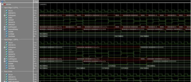
With all of this together, the interconnect functions as it should. Below is a screenshot of a successful run of the rv64gc arch64i regression test:
Frame Buffer
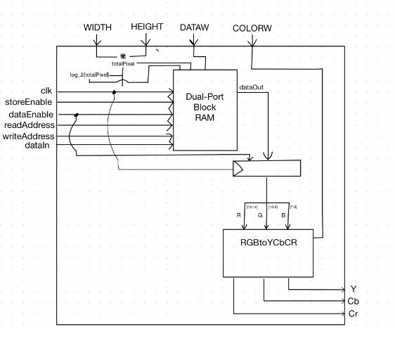
A frame buffer is required to store pixel data within a mapped area of random-access memory. Since we are developing the frame buffer for a field programable gate array, using the onboard block random access memory found on the VCU108 will accomplish the task while keeping the design simple and easy to control with the top-level module. The first several iterations of the frame buffer, included internal counters for the read and write addresses, but after testing the frame buffer in parallel with the signal generator, leaving the addressing to the top module helped eliminate frames from being overwritten before being pushed to the HDMI transmitter.
Since the VCU108 evaluation board only accepts YCbCr 4:2:2 pixel data, and the data stored within the CPU is kept in RGB, or red green blue, values, a color space converter is needed. Instead of using a board-specific IP to complete the conversion, shift registers can be used to accurately transfer the data to accepted values. More information regarding the individual modules found within the frame buffer and verification and testing can be found below:
Dual-port Block Random Access Memory
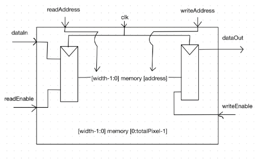
Block random access memory is used to store large amounts of data, and in this case, a specified amount of pixel data depending on the resolution desired from the video controller. Block RAM is a discrete part of an FPGA and has many different configuration options available based on the type of application. For our use case, inside of a frame buffer, the dual-port option is preferred, especially when synchronously reading and writing data. The difference between a single port and a dual-port is that a dual-port has the capability of two separate enables, clocks, and read and write addresses.
The ram module consists of two synchronous flip-flops which contain the read and write ports respectively. As seen below, each flip-flop is attached to the positive edge of a read and write clock, but while testing all of the modules together at the top level, it was simpler and accomplished the same results when tying both to a singular clock:
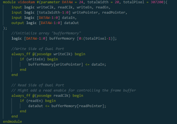
One issue which can happen when using block ram occurs when you try to read and write to the same address in memory on the same clock cycle can cause a previous output to output.
Color Conversion
Converting between RGB and YCbCr color values must occur because the only data type the VCU108 FPGA accepts is YCbCr 4:2:2 values. The difference between RGB and YCbCr is while RGB represents each color on a red, green, and blue basis, Y stands for the brightness, and Cb and Cr are data values with the brightness subtracted. The reason we suspect the FPGA manufacturer chose to have this as the only option is because it is easier for color processing and a human eyes perception.
To convert from RGB to YCbCr, instead of using an onboard intellectual property (IP), we decided to use the actual conversion equation found below and transfer them into a series of shift registers. This way our implementation of the video controller can be optimally used with different FPGA evaluation boards. When researching how to implement the shift registers, we found a beneficial open-source conversion application found below:


To test the shift register conversion, we used ModelSim to feed the module specific red, green, and blue values to test the accuracy of the implementation. The solved equations found below show the expected values for Y, Cb, and Cr and below, you can see the actual results from the simulation.
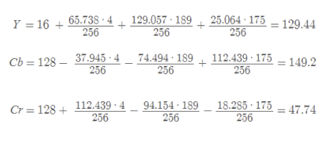
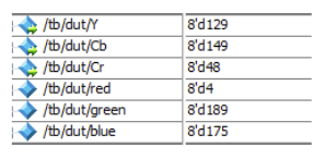
These results show a conversion accuracy of 99.5% compared to the expected conversion value.
Frame Buffer Testing and Results
For testing the frame buffer’s interaction with BRAM and the color conversion module, I created a Python script to generate an entire frame’s pixel data and passed the data through a test bench. As seen below, the light blue signal is the write enable, or data enable for the overall video controller design, and the purple signal is the read enable. The entire frame’s worth of data is loaded into the BRAM at specific bit mapped locations, and whenever the write enable is high, the address counter starts outputting the frame’s data.

The control of the frame buffer’s read and write addresses and enables happens within the top-level module since it is dependent on signals developed by the HDMI signal generator.
HDMI Signal Generator
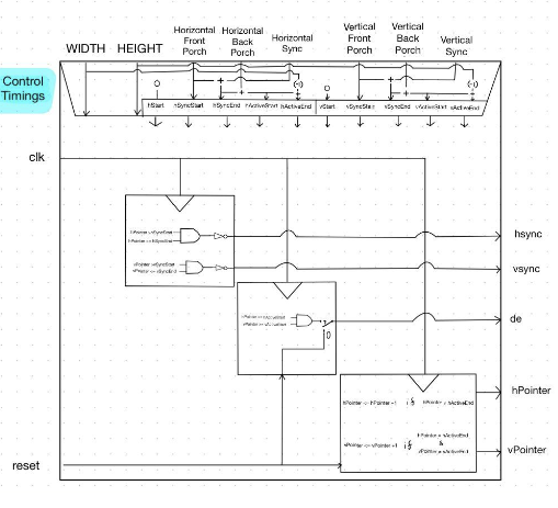
The HDMI signal generator is essential because it communicates with the HDMI transmitter where pixel data is located on a screen. Because every display is unique, with different pixel widths, heights, and blanking periods, the data signal must be controlled by timings to ensure the output video is clear and not deformed. By parameterizing each control timing in the top-level control module, the signals can adjust automatically to fit the distinctive application of the video controller. The required video waveforms produced by the module are data enable, horizontal sync, and vertical sync.
Control Timings
Handling the blanking periods of a display is required to control the location where data is pushed to a screen. As seen below, the timings can be broken down into front and back porches, and sync periods. The values of these periods are unique and based off the resolution and monitor operated. The control parameter values, when used with the horizontal and vertical positioning, tells the VSYNC, HSYNC, and data enable waveforms when they should be logic high, or logic low.

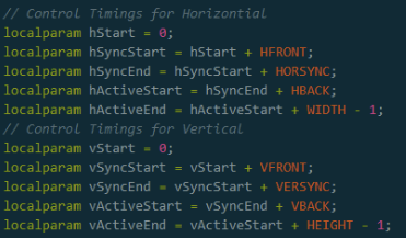
The local parameters shown above are based on the sync, porch, and active area sizes from the top-level module. The start and end times are used in correlation with the vertical and horizontal positioning. For horizontal and vertical sync signals, they are tied to a NAND gate to ensure the signal is only low during the syncing period and high when during the porches and active area. Data enable is tied to a AND gate which is high when both the vertical and horizontal signals are greater than or equal to the active area control timing.
Vertical and Horizontal Positioning
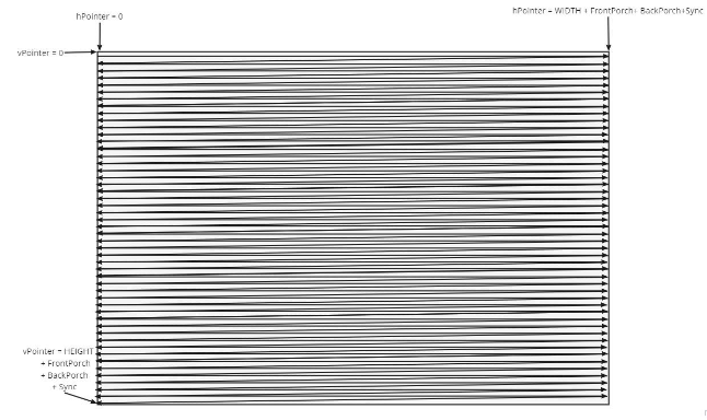
The vertical and horizontal counter is essential to control the generator’s signals, as well as helping to ensure the video controller is operating on the same controls. The size of both the vertical and horizontal pointers is determined by the size of the frame buffer needed to display to an established resolution plus the blanking period times. The way pixels are written to a screen is shown below. Starting in the top left corner of the screen, the pixels are displayed from left to right, one line at a time. Once reaching the active end of the horizontal axis, the vertical counter is incremented, and the horizontal counter is reset. This process is repeated until the pointer is at the active end for both vertical and horizontal counters. Both counters are then reset, and a new frame begins at the top left position.
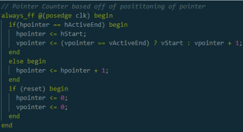
Shown above, is the application of the counters being controlled by timing parameters, and below is the simulation results in ModelSim.

Signal Generator Testing and Results
Since the signal generator is just creating output signals, with the only inputs being reset and the clock, testing the signal generator was a combination of verifying the control timings were working correctly and comparing the waveforms to the expected waveforms of the ADV7511 HDMI Transmitter chip. Using a video timings calculator, we used the suggested porch and sync timings for the resolution we used to test the signal generator. The waveforms shown below display HSYNC, in the pink waveform, VSYNC, in the orange waveform, and data enable, in the teal waveform, signals for an entire frame at VGA resolution.


hown above are the expected transmitter signal waveforms, found within the ADV7511 Programming Guide, and the actual waveforms from the ModelSim simulation.
Top Level Frame and Signal Control
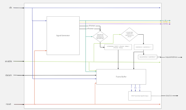
The top control module helps combine both the signal generator and frame buffer sections of the video controller and sends data and control signals to the HDMI transmitter chip to push a display onto a screen. The diagram above displays the control logic which makes sure pixel data is correctly outputted to the transmitter. The module uses the pixel position on the screen to control which pixels are supposed to be displayed. Shown below is how the horizontal and vertical pointer location is used to find wherein the frame buffer the data is located.
![]()
Whenever the pointers are within the active area and data enable is high, the write address is calculated and used by the frame buffer to output the data stored within the BRAM in the frame buffer and then pushed to the HDMI transmitter chip. The requested address is used to communicate with the AHB system to load the next address needed to be read and stored in the frame buffer. When the enable from the AHB system is high, the read address will start incrementing.

Since the AHB system was not finished in time to test the video controller interactions with the CPU, a pixel bank was used to store an entire frame’s worth of RGB data. As seen above, all the components interact with each other correctly as expected and output data only during the active area of the signal generator and in the correct order.
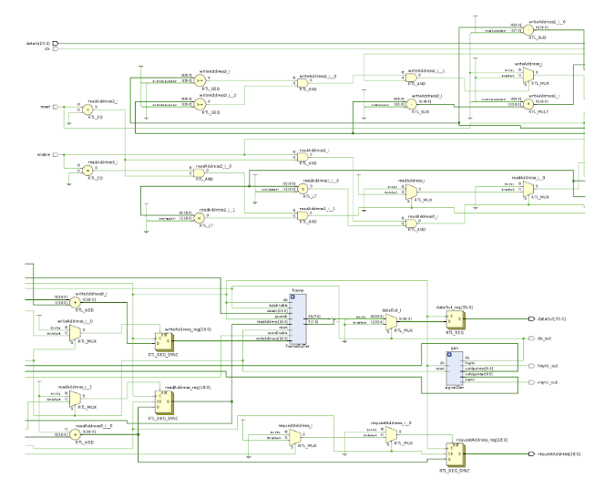
After testing the top-level module at different resolutions to verify the design is expandable and still operates properly, we were able to synthesize the design on Xilinx Vivado for the VCU108 evaluation board to receive the RTL schematic for the design as shown above.
ADV7511 HDMI Transmitter Chip
The VCU108 includes an ADV7511 HDMI Transmitter Chip which we use to turn the output of the video signal generator into a proper HDMI signal. Before the transmitter will output anything, it must be programmed through a series of internal register writes through its I2C interface. These register values represent information about input color space, resolution, and timing. Additional registers on the transmitter can be used to configure advanced HDMI features such as audio and content protection, but our project does not make use of these.
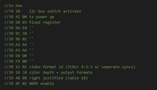
The first data packet is used to configure the TCA9548 I2C Switch that the VCU108 uses to isolate its I2C peripherals. The value 0x20 configures the switch to allow communication only with the HDMI transmitter. The next 8 packets are referred to as ‘fixed registers’ by the ADV7511 programming manual and must be set to a pre-defined value on startup.
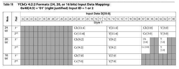
The next packet tells the transmitter the input of the format signal. Register 0x15 uses the upper half-byte to configure I2S audio, which here we disable by setting to 0. The lower half-byte sets the input format to be YCbCr 4:2:2 with separate syncs. Registers 0x16 and 0x48 are then set to the value representing 16-bit input in the format shown below. The connection of the HDMI transmitter forced us into using this video format. Only bits 8 through 23 are physically connected on the VCU108, and only this input mode supports such a configuration.
Finally, the last data packet activates the transmitter output with the configured settings. This register can also be used to configure the transmitter to act as a DVI source rather than an HDMI source, and we had planned to utilize this option to avoid potential licensing issues that could come with making use of HDMI IP. This option was not implemented due to time constraints.
I2C Controller
To interface with the HDMI transmitter, we needed an I2C controller. I2C is an extremely standard serial communication bus, and we compared several possible implementations for our project. The first option considered was using Xilinx IP. This would have involved running a MicroBlaze soft processor core on the FPGA alongside Wally, and this core could then make requests over an AXI Bus which could then interface with the system I2C bus through another IP Block. However, this method presented some challenges that made it impractical. Reliance on additional IP makes the project less reusable for the ongoing Wally project. We also considered the additional challenge of learning a new toolchain to interact with this processor, as the project had already experienced delays related to research and training with new tools and workflows.
The second option considered was using an open-source I2C controller. Multiple candidates were considered, and all of them had similar issues. These controllers contained overhead for various control methods, the most common being the open-source Wishbone interface. Like the previous option, this would require learning an entirely new standard, which would delay the project further. Additionally, reverse engineering the cores to remove this overhead required about as much work as implementing a core of our own. The final option, which was selected for the project, was to write our own I2C controller from scratch. This option presented several advantages, such as ease of integration and the ease of expanding with additional features as the project went along.
The core idea of the design was to implement two cooperating state machines which would read the data packets from memory and iterate through them with the appropriate I2C signals. The first state machine, called the bit state machine, kept track of what kind of signal the controller was sending at that time. The five states were IDLE, START, STOP, READ, and WRITE. These states cause the controller to do nothing, send the I2C start signal by pulling SDA low then pulling SCL low, send the I2C stop signal by releasing the SCL line then releasing the SDA line, read one bit, or write one bit, respectively.
To meet the necessary timing requirements, each of these states was divided into 4 or 5 substates, which update on each clock tick. These substates contain logic which updates several pointers, which represent the current position within memory, the position within the I2C data frame, and the position within the current byte. Each substate assigns some output value for SDA and SCL, but not directly. Because the I2C bus is pulled up externally, we must use a tri-state buffer to prevent the FPGA from sourcing current. The output is in a high impedance state when we want the bus to be high, and 0 when we want to pull it low.


Wally Running on VCU108
The Wally processor has in the past been run on the VCU118 evaluation board by the research groups working on it. Since the VCU108 uses the same design tools and workflow, we were able to modify the existing configuration files for the VCU118 to work on our board. To do this, we changed the main constraints file that the Xilinx Vivado file uses to assign top level ports in the design to physical pins on the FPGA by referencing the user guide for the board. Additionally, the VCU118 implementation makes use of Xilinx IP to interface between Wally and peripherals on the board, such as the DDR4 RAM which Wally uses as its main memory. This IP was mostly integrated without extensive modification because the Vivado workflow recompiles these for the target board as part of the build process. Some changes were needed to account for the differing clock speeds between the two boards.
The VCU108 has a different set of internal clocks that run at different frequencies than the clocks on the VCU118 board. The DDR4 interface contains an internal clock divider which took the 250 MHz main clock on the VCU118 and turned it into 2 slower clocks: a 22 MHz clock to drive Wally and the AHB Bus, and a 208 MHz clock that drives the DDR4 memory interface. The parameters for these dividers were set in a TCL file and were altered to accept the VCU108’s 300 MHz main clock. Confusion about these clock dividers lead to a major halt in the development process because the mismatch in clock frequency between the boards caused the serial UART system to have improper timing.
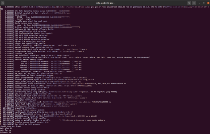
Once the timing issues were resolved, we were able to boot a version of the Linux kernel that was compiled specifically for Wally. The output of the kernel boot sequence was monitored through Wally’s UART port. The boot sequence gets most of the way through the process but is interrupted by a kernel-panic near the end. This causes the boot sequence to loop forever. Resolving this issue was outside the scope of our project.
